Learning
The 555 timer is a simple integrated circuit that can be used to make many different electronic circuits. With this information you will learn how how the 555 works and will have the experience to build some of the circuits below.
An Overview of the 555 Timer
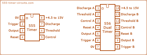
The 555 Integrated Circuit (IC) is an easy to use timer that has many applications. It is widely used in electronic circuits and this popularity means it is also very cheap to purchase, typically costing around 30p. A 'dual' version called the 556 is also available which includes two independent 555 ICs in one package.The following illustration shows both the 555 (8-pin) and the 556 (14-pin).
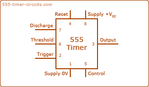
In a circuit diagram the 555 timer chip is often drawn like the illustration below. Notice how the pins are not in the same order as the actual chip, this is because it is much easier to recognize the function of each pin, and makes drawing circuit diagrams much easier.
For the 555 to function it relies on both analogue and digital electronic techniques, but if we consider its output only, it can be thought of as a digital device. The output can be in one of two states at any time, the first state is the 'low' state, which is 0v. The second state is the 'high' state, which is the voltage Vs (The voltage of your power supply which can be anything from 4.5 to 15v. 18v absolute maximum). The most common types of outputs can be categorized by the following (their names give you a clue as to their functions):
- Monostable mode: in this mode, the 555 functions as a "one-shot". Applications include timers, missing pulse detection, bouncefree switches, touch switches, frequency divider, capacitance measurement, pulse-width modulation (PWM) etc
- Astable - free running mode: the 555 can operate as an oscillator. Uses include LED and lamp flashers, pulse generation, logic clocks, tone generation, security alarms, pulse position modulation, etc.
- Bistable mode or Schmitt trigger: the 555 can operate as a flip-flop, if the DIS pin is not connected and no capacitor is used. Uses include bouncefree latched switches, etc.
Pin Configuration of the 555 Timer
Here is the identification for each pin: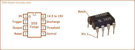
When drawing a circuit diagram, always draw the 555 as a building block, as shown below with the pins in the following locations. This will help you instantly recognise the function of each pin:
Pin 1 (Ground):
Connects to the 0v power supply.
Pin 2 (Trigger):
Detects 1/3 of rail voltage to make output HIGH. Pin 2 has control over pin 6. If pin 2 is LOW, and pin 6 LOW, output goes and stays HIGH. If pin 6 HIGH, and pin 2 goes LOW, output goes LOW while pin 2 LOW. This pin has a very high impedance (about 10M) and will trigger with about 1uA.
Pin 3 (Output):
(Pins 3 and 7 are "in phase.") Goes HIGH (about 2v less than rail) and LOW (about 0.5v less than 0v) and will deliver up to 200mA.
Pin 4 (Reset):
Internally connected HIGH via 100k. Must be taken below 0.8v to reset the chip.
Pin 5 (Control):
A voltage applied to this pin will vary the timing of the RC network (quite considerably).
Pin 6 (Threshold):
Detects 2/3 of rail voltage to make output LOW only if pin 2 is HIGH. This pin has a very high impedance (about 10M) and will trigger with about 0.2uA.
Pin 7 (Discharge):
Goes LOW when pin 6 detects 2/3 rail voltage but pin 2 must be HIGH. If pin 2 is HIGH, pin 6 can be HIGH or LOW and pin 7 remains LOW. Goes OPEN (HIGH) and stays HIGH when pin 2 detects 1/3 rail voltage (even as a LOW pulse) when pin 6 is LOW. (Pins 7 and 3 are "in phase.") Pin 7 is equal to pin 3 but pin 7 does not go high - it goes OPEN. But it goes LOW and will sink about 200mA.
Pin 8 (Supply):
Connects to the positive power supply (Vs). This can be any voltage between 4.5V and 15V DC, but is commonly 5V DC when working with digital ICs.
Inside the 555 Timer
You may wonder what is inside the 555 timer chip or what makes it work. Well, the 555 timer chip an Intergrated Circuit (IC) and therefore it contains a miniturized circuit surrounded by silicon. Each of the pins is connected to the circuit which consists of over 20 transistors, 2 diodes and 15 resistors.
The illustration below shows the functional block diagram of the 555 timer IC.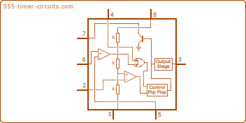
Do you notice the three 5k resistors? This is how the chip got it's name.555 Timer Operating Modes
The 555 has three main operating modes, Monostable, Astable, and Bistable. Each mode represents a different type of circuit that has a particular output.
Astable mode
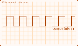
An astable circuit has no stable state - hence the name "astable". The output continually switches state between high and low without without any intervention from the user, called a 'square' wave. This type of circuit could be used to give a mechanism intermittent motion by switching a motor on and off at regular intervals. It can also be used to flash lamps and LEDs, and is useful as a 'clock' pulse for other digital ICs and circuits.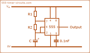
Monostable mode
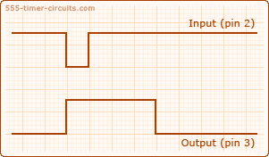
A monostable circuit produces one pulse of a set length in response to a trigger input such as a push button. The output of the circuit stays in the low state until there is a trigger input, hence the name "monostable" meaning "one stable state". his type of circuit is ideal for use in a "push to operate" system for a model displayed at exhibitions. A visitor can push a button to start a model's mechanism moving, and the mechanism will automatically switch off after a set time.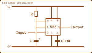
Bistable Mode (or Schmitt Trigger)
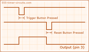
A bistable mode or what is sometimes called a Schmitt Trigger, has two stable states, high and low. Taking the Trigger input low makes the output of the circuit go into the high state. Taking the Reset input low makes the output of the circuit go into the low state. This type of circuit is ideal for use in an automated model railway system where the train is required to run back and forth over the same piece of track. A push button (or reed switch with a magnet on the underside of the train) would be placed at each end of the track so that when one is hit by the train, it will either trigger or reset the bistable. The output of the 555 would control a DPDT relay which would be wired as a reversing switch to reverse the direction of current to the track, thereby reversing the direction of the train.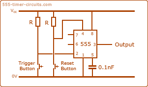
Using the Output of a 555 Timer
The output (Pin 3) of the 555 can be in one of two states at any time, which means it is a digital output. It can be connected directly to the inputs of other digital ICs, or it can control other devices with the help of a few extra components. The first state is the 'low' state, which is the voltage 0V at the power supply. The second state is the 'high' state, which is the voltage Vcc at the power supply.
Sinking and Sourcing
When the Output goes low, current will flow through the device and switch it on. This is called 'sinking' current because the current is sourced from Vs and flows through the device and the 555 to 0V.
When the Output goes high, current will flow through the device and switch it on. This is called 'sourcing' current because the current is sourced from the 555 and flows through the device to 0V.
Sinking and sourcing can also be used together so that two devices can be alternately switched on and off.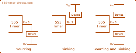
The device(s) could be anything that can be switched on and off, such as LEDs, lamps, relays, motors or electromagnets. Unfortunately, these devices have to be connected to the Output in different ways because the Output of the 555 can only source or sink a current of up to 200mA. Make sure your power supply can provide enough current for both the device and the 555, otherwise the timing of the 555 will be affected.Common Mistakes When Using a 555 Timer
Here are some mistakes to avoid:
1. Pin 7 gets connected to the 0v rail via a transistor inside the chip during part of the operation of the 555. If the pot is turned to very low resistance in the following circuit, a high current will flow through the pot and it will be damaged:
2. The impedance of the 100u electrolytic will allow a very high current to flow and the chip will get very hot. Use 10u maximum when using 8R speaker.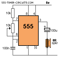
3. The reset pin (pin 4) is internally tied HIGH via approx 100k but it should not be left floating as stray pulses may reset the chip.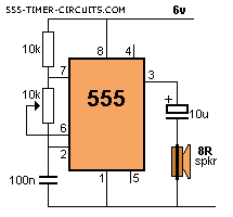
4. Do not draw 555 circuits as shown in the following diagram. Keep to a standard layout so the circuit is easy to follow.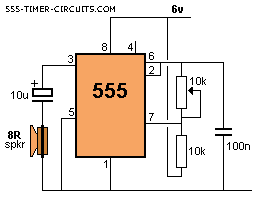
5. Here's an example from the web. It takes a lot of time to work out what the circuit is doing: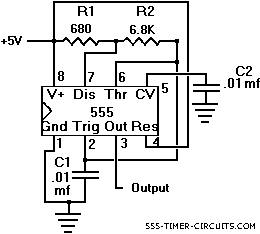
The aim it to lay-out a circuit so that it shows instantly what is happening. That's why everything must be in recognised locations.
Here is the corrected circuit: From this diagram it is obvious the circuit is an oscillator (and not a one-shot etc).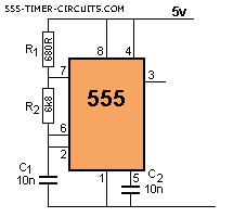
6. Don't use high value electrolytics and high resistances to produce long delays. The 555 is very unreliable with timing values above 5-10 minutes. The reason is simple. The charging current for the electrolytic is between 1 - 3 microamp in the following diagram (when the electro is beginning to charge) and drops to less than 1 microamp when the electro is nearly charged.
If the leakage of the electro is 1 microamp, it will never fully charge and allow the 555 to "time-out."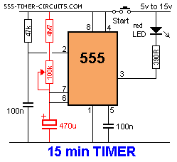
7. Do not connect a PNP to the output of a 555 as shown in the following diagram. Pin 3 does not rise high enough to turn off the transistor and the current taken by the circuit will be excessive. Use an NPN driver.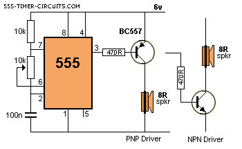
Tidak ada komentar:
Posting Komentar